

 español



La conexión entre PCB e IA (parte complementaria)
Anteriormente, aclaramos la lógica de valor, el crecimiento del mercado, la estratificación del producto y los requisitos de actualización tecnológica provocados por la iteración de módulos ópticos de alta velocidad para PCB en la era de la IA, y esbozamos los dividendos industriales de las placas base y backplanes de alta velocidad. Sobre esta base, este artículo realiza una adición clave: el verdadero núcleo de alto valor y la vía de alta barrera en la IA y cadena de la industria de PCB no son las placas convencionales de alta velocidad, sino más bien sustratos de empaquetado de CI, que han sido subestimados durante mucho tiempo y determinan directamente el límite superior de la capacidad de producción de potencia informática de gama alta.
Es la plataforma de soporte central para chips de IA, GPU y memoria HBM. No solo es la barrera tecnológica más crítica para el hardware informático, sino también la vía de alto valor más prometedora para la sustitución nacional en la cadena actual de la industria de la IA.
Si una PCB normal es el "esqueleto" de un producto electrónico, entonces el sustrato de empaquetado es el "portador íntimo" del chip, también conocido como la segunda placa de circuito del chip. Sirve como convertidor de señal entre los diminutos pines del chip y los circuitos de la placa base, y es un material central indispensable en el proceso de empaquetado de chips.
En comparación con las PCB ordinarias, las barreras tecnológicas de los sustratos de empaquetado son abrumadoramente más altas. Las PCB ordinarias tienen un ancho de línea mínimo de solo 50 μm, mientras que los procesos avanzados utilizados en los sustratos de empaquetado pueden lograr anchos de línea tan bajos como 2 μm. Combinado con una estructura de apilamiento de precisión de 2-20 capas, esto requiere el uso de procesos semiaditivos SAP/mSAP de gama alta para la producción. Este umbral tecnológico extremadamente alto también mantiene el margen de beneficio bruto de la industria estable en un 30%-40%, superando con creces al de los productos de PCB tradicionales.
Actualmente, los sustratos de empaquetado convencionales se dividen en dos categorías principales: ABF y BT. La estructura del mercado está claramente definida y ha estado monopolizada durante mucho tiempo por empresas extranjeras.
El sustrato ABF es un material central esencial para la potencia informática de IA de gama alta, con barreras tecnológicas extremadamente altas. Este material se desarrolla exclusivamente en Japón y se suministra a nivel mundial, y con sus capacidades de cableado ultrafino y apilamiento multicapa, está diseñado específicamente para empaquetar chips de potencia informática de IA de gama alta como GPU y CPU.
Japón ha monopolizado básicamente la capacidad de producción global de ABF de gama alta, y China solo ha logrado una verificación preliminar de producción en masa. La tasa de localización de sustratos adaptadores de chips de IA de gama alta es inferior al 10%, lo que la convierte en una de las vías de "cuello de botella" más críticas en el campo actual de los semiconductores.
Los sustratos BT están orientados al campo de los semiconductores de consumo, centrándose en una alta resistencia al calor y siendo ampliamente utilizados en productos como SoC móviles, memoria y módulos de RF. En comparación con los sustratos ABF, los sustratos BT tienen una menor dificultad de fabricación y una localización más rápida. Aunque el sustrato central sigue estando controlado por empresas japonesas y taiwanesas, los fabricantes nacionales han logrado una sustitución masiva, reduciendo significativamente la presión de los cuellos de botella tecnológicos.
Las triples barreras de la tecnología de procesos, los clientes y la certificación son las razones principales del monopolio a largo plazo de las empresas extranjeras. El aumento del rendimiento de la producción de circuitos ultrafinos es extremadamente difícil, y el sustrato debe estar estrechamente adaptado al diseño del fabricante del chip. Cambiar de proveedor requiere una revisión completa de la solución del chip, lo que resulta en una lealtad del cliente extremadamente fuerte. Además, entrar en la cadena de suministro de los líderes internacionales requiere un estricto ciclo de certificación de 3 a 5 años. Las sólidas barreras de los primeros participantes mejoran aún más la escasez de avances tecnológicos por parte de los principales fabricantes nacionales.
Hoy en día, la industria de PCB ha superado hace mucho tiempo la era dominada por los teléfonos inteligentes y las PC. El mercado tradicional de electrónica de consumo está experimentando un crecimiento estancado, sobrecapacidad y una feroz competencia por los beneficios. Mientras tanto, los tres sectores de gama alta de servidores de IA, vehículos de nueva energía y comunicaciones 5G se han convertido en los motores centrales del crecimiento de la industria, transformando completamente la industria de modelos de "bajo precio y alto volumen" a modelos de "alto precio y alto valor añadido".
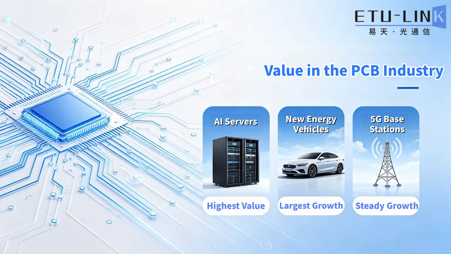
1.Servidores de IA: mayor valor, más rápido crecimiento
Esta es actualmente el área central de más rápido crecimiento y mayor valor en la industria de PCB. La carrera armamentista mundial por la potencia informática de IA continúa intensificándose, y los servidores de gama alta se iteran constantemente. El valor de PCB de un solo servidor de IA de nivel H100 puede alcanzar entre 3.000 y 5.000 dólares, lo que es casi 10 veces mayor que el de un servidor normal.
Los servidores de IA de gama alta requieren placas multicapa de ultra alto rendimiento con más de 20 capas y materiales especiales de alta frecuencia y alta velocidad, lo que los hace extremadamente exigentes técnicamente. A medida que los modelos de IA a gran escala continúan expandiéndose y las demandas de potencia informática siguen aumentando, la demanda incremental de PCB de gama alta y sustratos de empaquetado seguirá creciendo a largo plazo.
2.Vehículos de nueva energía: el sector con mayor potencial de crecimiento
La penetración acelerada de los vehículos eléctricos e inteligentes ha aumentado significativamente el valor de la PCB automotriz por vehículo. Los vehículos de gasolina tradicionales tienen una estructura simple, con un valor de PCB de solo alrededor de 200 dólares por vehículo; mientras que los vehículos de nueva energía están equipados con módulos centrales como el sistema de tres componentes eléctricos, cabina inteligente, radar de vehículo y conducción autónoma, lo que aumenta directamente el valor de la PCB por vehículo a 400-600 dólares.
Mientras tanto, los productos de grado automotriz tienen requisitos estrictos de fiabilidad y estabilidad, y la barrera de entrada extremadamente alta evita la competencia de gama baja, lo que convierte a las PCB automotrices en una vía central con un amplio crecimiento incremental y una alta rentabilidad.
3. Estación base 5G: Robusta gama alta Plataforma
Las PCB de comunicación forman la base del crecimiento estable de la industria. Las estaciones base 5G tienen una demanda rígida de PCB de alta frecuencia y alta velocidad; una sola PCB de estación base puede tener un valor de $1,500-$3,000, y el precio unitario de los laminados revestidos de cobre de alta frecuencia utilizados es de 5 a 10 veces mayor que el de las placas ordinarias, lo que resulta en un valor añadido extremadamente alto. Con la recuperación del ciclo de construcción nacional de 5G y el avance continuo de la investigación y el desarrollo de tecnología 6G prospectiva, la demanda de PCB de comunicación de alta gama está aumentando constantemente, proporcionando un soporte de rendimiento continuo y robusto para la industria.
En la era de la IA, la fabricación de PCB ya no es una industria tradicional de bajo valor añadido. La lógica central de la industria es clara: la competencia interna por materiales de placa de gama baja y la consolidación de beneficios, junto con Sustitutos nacionales para sustratos de embalaje y Aumento en tres demandas principales de alta gama, serán los principales motores de crecimiento para la industria en los próximos 3-5 años.
Las prioridades de demanda también son muy claras:
Los servidores de IA, con su alto valor y alta tasa de crecimiento, ocupan firmemente el primer lugar; los vehículos de nueva energía les siguen de cerca con un crecimiento masivo del mercado; la comunicación 5G se basa en altas barreras para construir una base sólida; y los dividendos industriales de las PCB de alta gama se están liberando a un ritmo acelerado.
Este artículo complementa de manera integral las barreras tecnológicas y las ventajas competitivas de la industria de PCB, con la esperanza de proporcionarle una referencia sustancial. Si encuentra útil el contenido, ¡por favor dele a me gusta y guárdelo! Continuaremos enfocándonos en el sector de la comunicación óptica , actualizando continuamente los conocimientos básicos sobre iteraciones de la industria, avances tecnológicos y sustitución nacional, ayudándole a aprovechar continuamente las oportunidades en este campo. ¡Bienvenido a seguirnos!
Categorías
nuevo blog
Etiquetas
nuevos productos
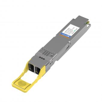
Transceptor óptico 800G OSFP 2×DR4 1310nm 500M MPO12 DDM Lee mas
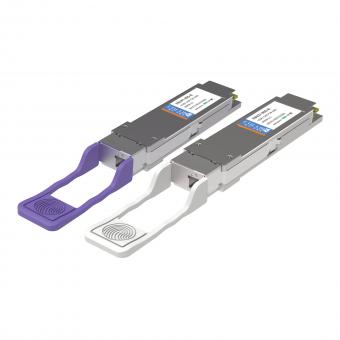
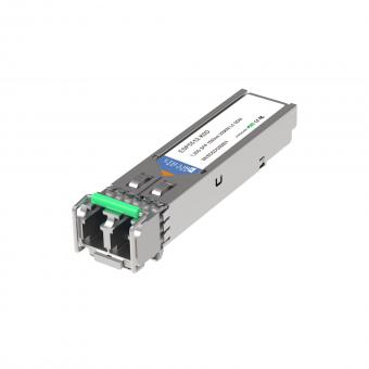
Transceptor óptico LC SFP de 1,25 G, 1550 nm y 200 km Lee mas
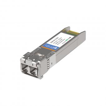

Transceptor óptico LC de 100G QSFP28 LR con sonda Lambda única de 10KM Lee mas
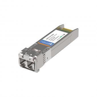
Transceptor óptico de 25G SFP28 ZR 1310nm los 80KM LC Lee mas
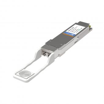
Transceptor óptico de generación II de 100G QSFP28 ZR4 80KM LC Lee mas
Para consultas sobre nuestros productos o lista de precios, déjenoslo y nos pondremos en contacto dentro de las 24 horas.


 13th Floor, Building 6, Honghualing Base, Nanshan Intelligent Manufacturing Base, Liuxian Avenue, Taoyuan Street, Xili, Nanshan District, Shenzhen, China
© Derechos de autor: 2026 ETU-Link Technology CO ., LTD Reservados todos los derechos.

Soporta red IPv6


